|Home|Research|Industry|Education|Contacts|
| Examples of Plasma Processing: Etching features on Micro - Electronics Chips Surface Preparation of Potatoe Chip Bags for Printing Thermal Coatings for Jet Engine Blades Hard Coatings for Metal Cutting Tools and Dies |
Plasma-Aided ManufacturingPlasma-aided manufacturing (or Plasma Processing), the use of electrically charged particles in the manufacturing process, is used for producing new materials with unusual and superior properties. It also is used for developing new chemical compounds and processes, machining, as well as altering and refining various materials and surfaces. Plasma-aided manufacturing has direct applications in semiconductor fabrication, materials, synthesis, welding, lighting, polymers, waste removal, high-performance ceramics, and numerous other items in both high-technology and the more "traditional" manufacturing processes. A plasma is formed by adding energy to a gas, causing it to break up into ions and electrons. In this ionized state, the gas is electrically conductive. Plasmas are often called the fourth state of matter--after solids, liquids, gases--since in each state, adding energy will cause a transformation to the next state. In industry, two types of plasmas are used. Glow discharge plasmas, like those seen in neon signs operate at low pressure. Thermal plasmas, which occur in lightning and electrical arcs, are produced at atmospheric pressure. The versatility of plasmas for manufacturing has been known for some time. Yet the ability to exploit them in the manufacturing environment has remained limited because of the lack of process control for specific applications. Rapid advancement in this emerging technology will help the United States recapture its industrial market share in microelectronics, high-temperature ceramics, machine tools, and other industries. |
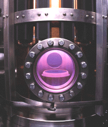
Inductively coupled plasma source with magnetic bucket confinement for plasma etching. MRFI (Magnetic Radio Frequency Inductive) source. Photo by Bruce Fritz.
|Home|Research|Industry|Education|Contacts|
 |
Last Modified: Friday,
August 22, 1997 02:39 PM This page is best viewed by browsers that support background colors in tables. All photographs © 1997 Engineering Research Center for Plasma-Aided Manufacturing. Address comments to ercpam@silver.neep.wisc.edu |